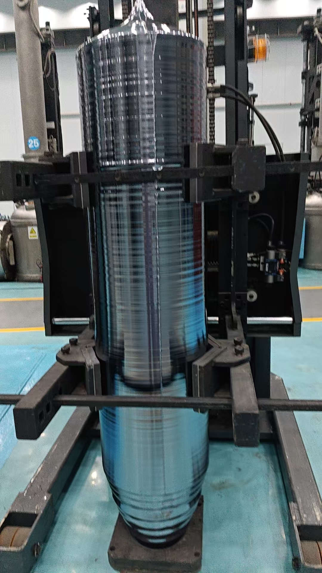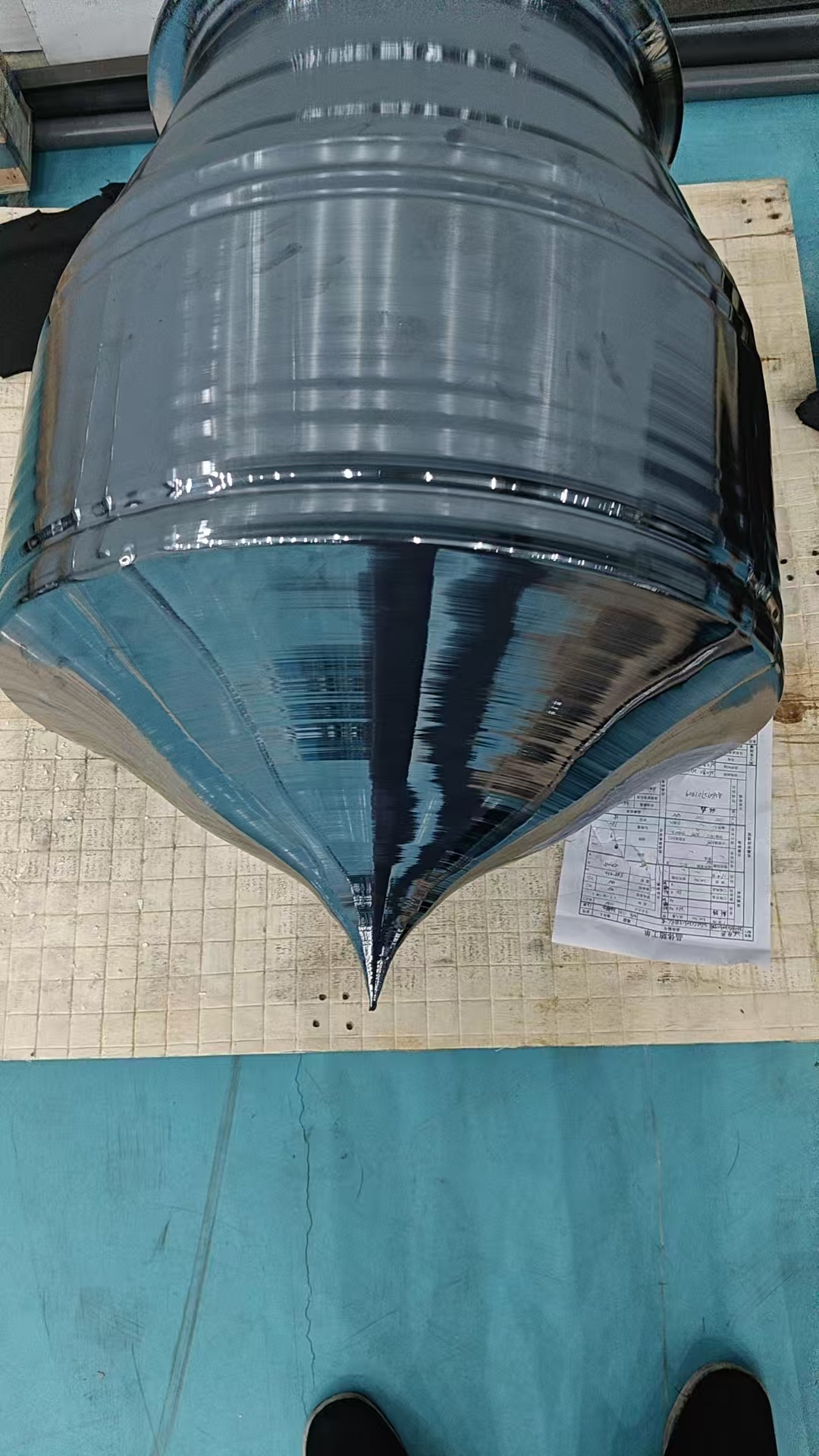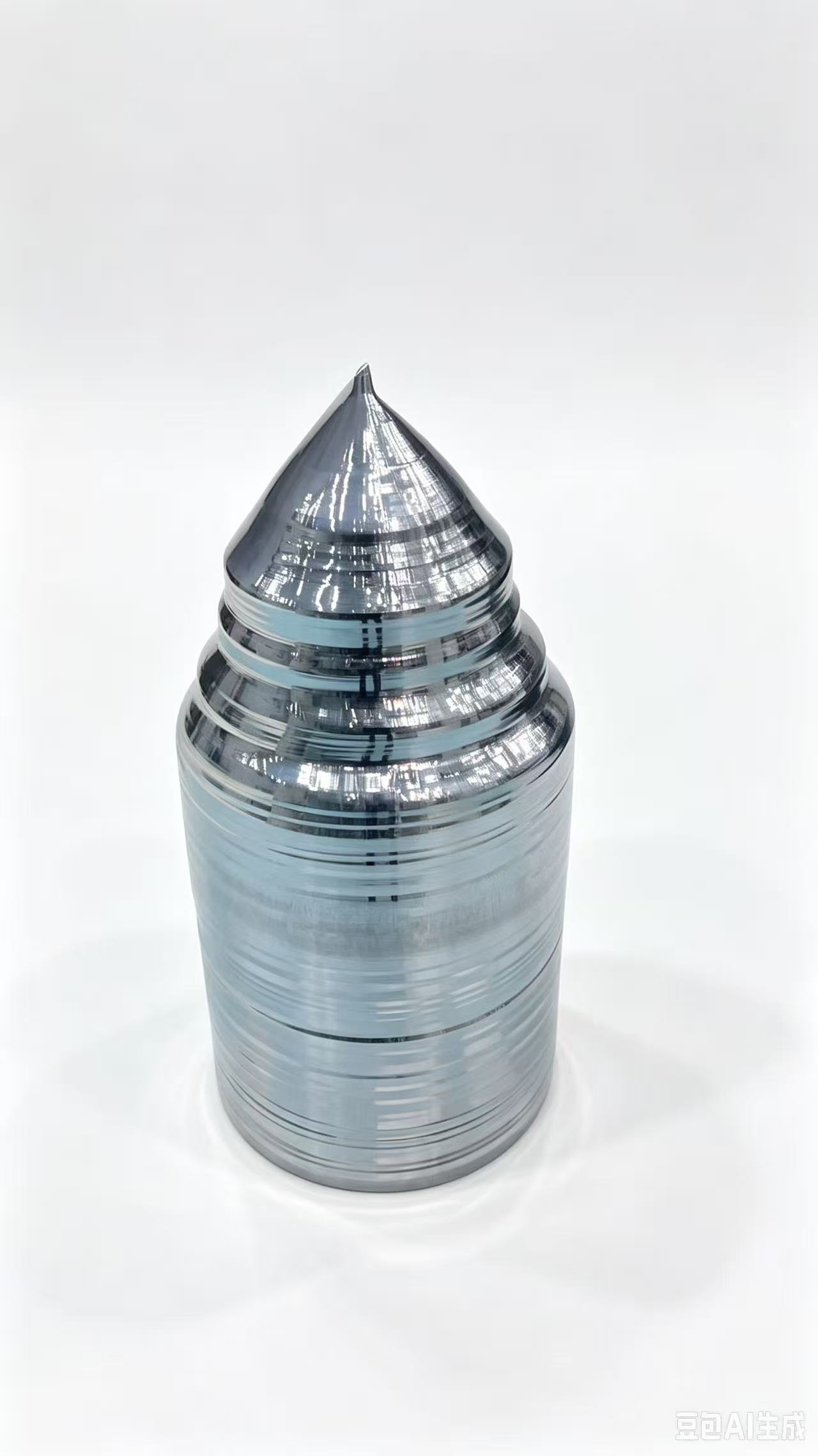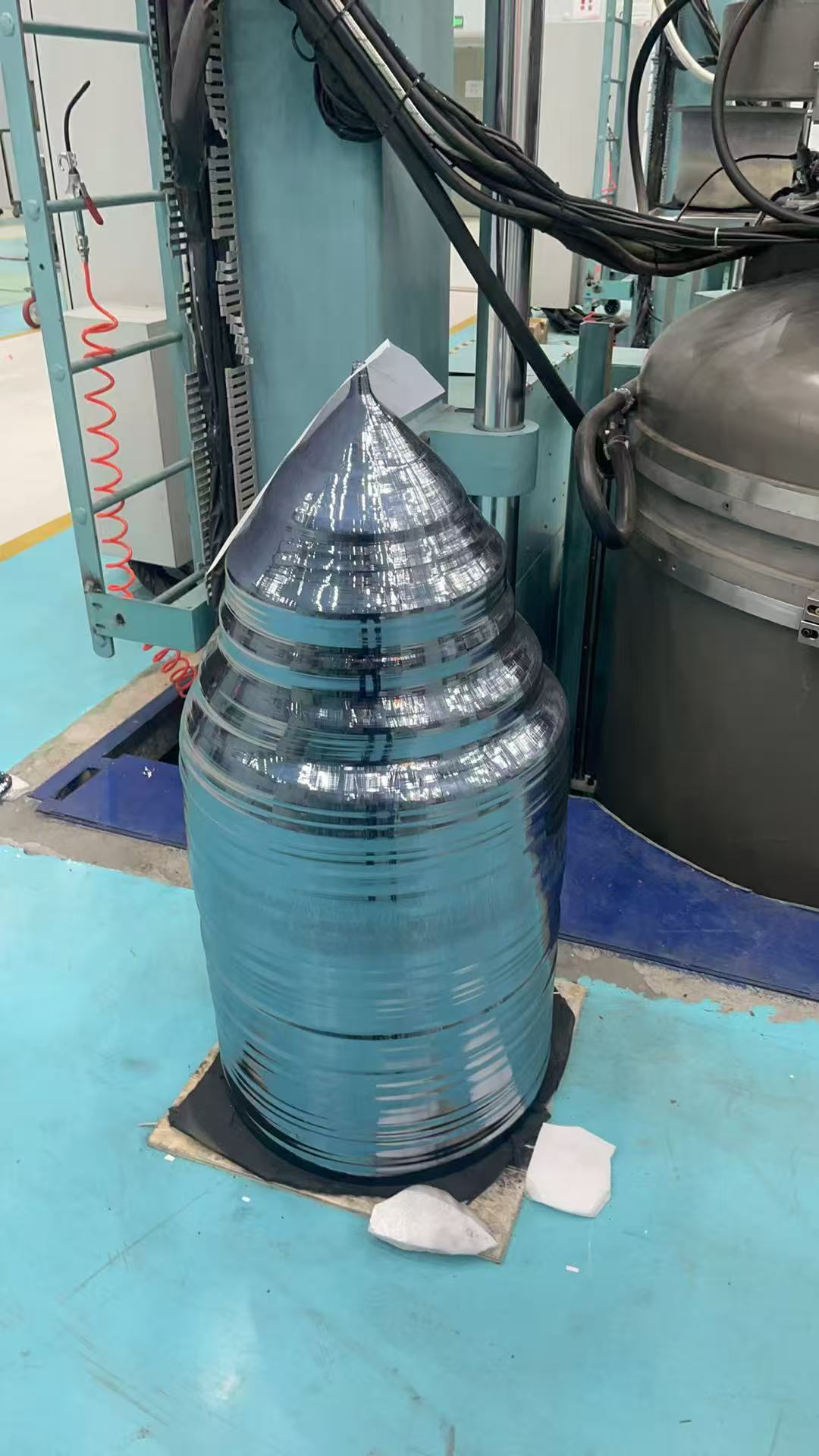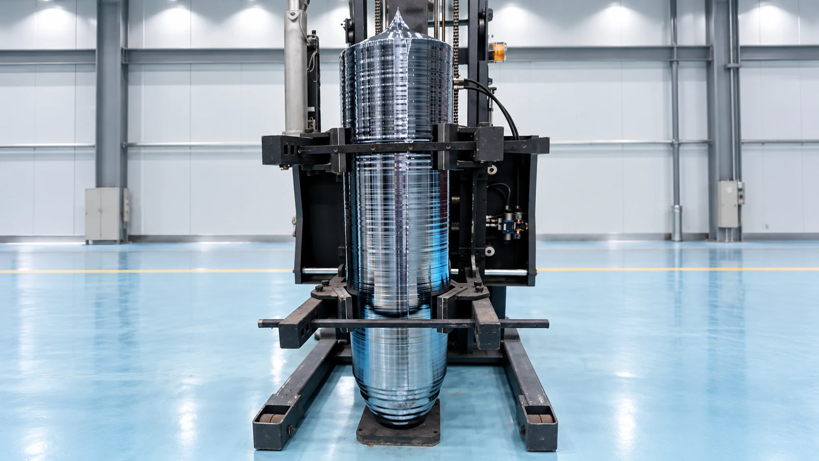
Large-Diameter Crystal Technology
CZ growth of large-diameter monocrystalline silicon, with process control for crystal dimensions, conductivity type and resistivity.
Learn More
CZ growth of large-diameter monocrystalline silicon, with process control for crystal dimensions, conductivity type and resistivity.
Learn More
Define machining allowances against component drawings. Sizing, cropping and coring create silicon ingots, cylinders and rings.
Learn More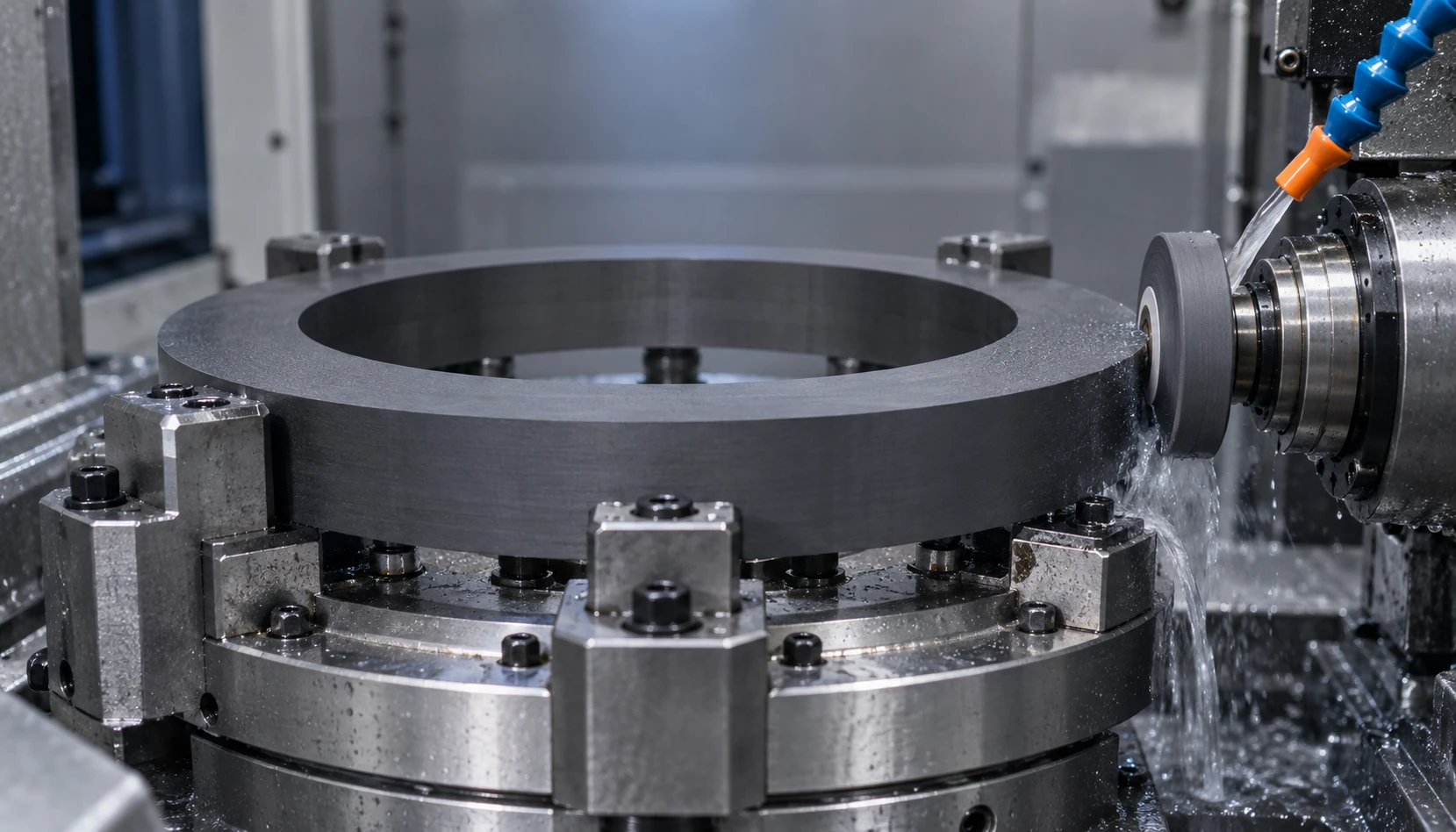
Cutting, grinding and precision machining address critical dimensions, tolerances and surface condition. Delivery requirements follow the technical agreement.
Learn More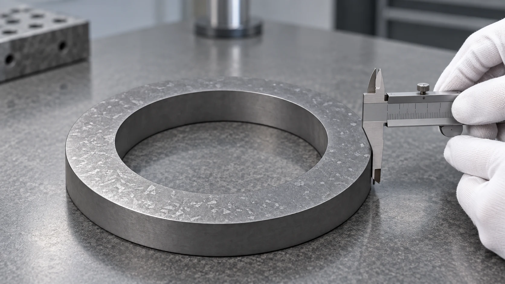
Define test items and acceptance criteria for material properties, critical dimensions and surface condition, then inspect under the technical agreement.
Learn More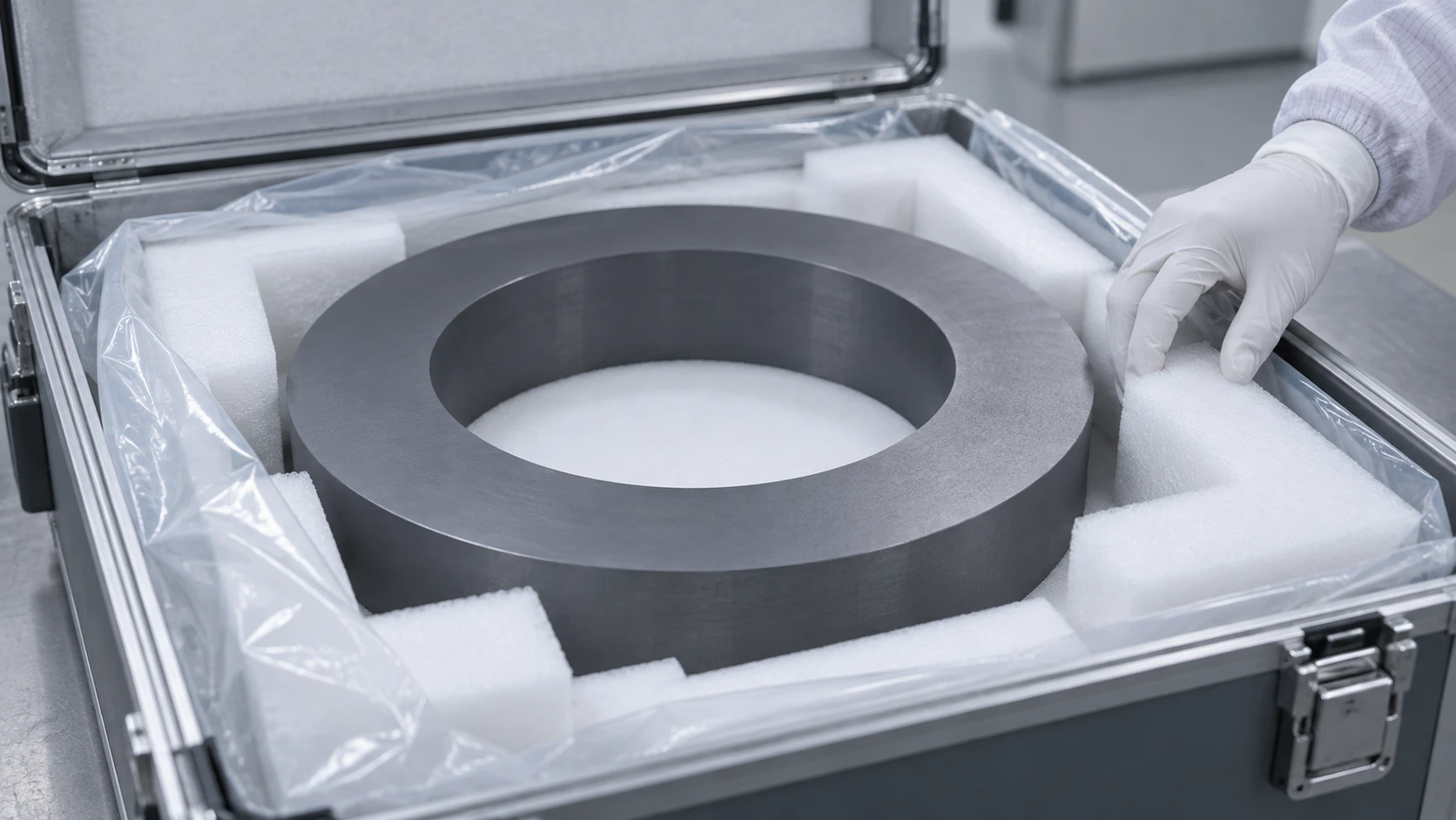
Arrange cleaning, protection, packaging and identification according to the material form and transport needs, with the required delivery documents.
Learn More