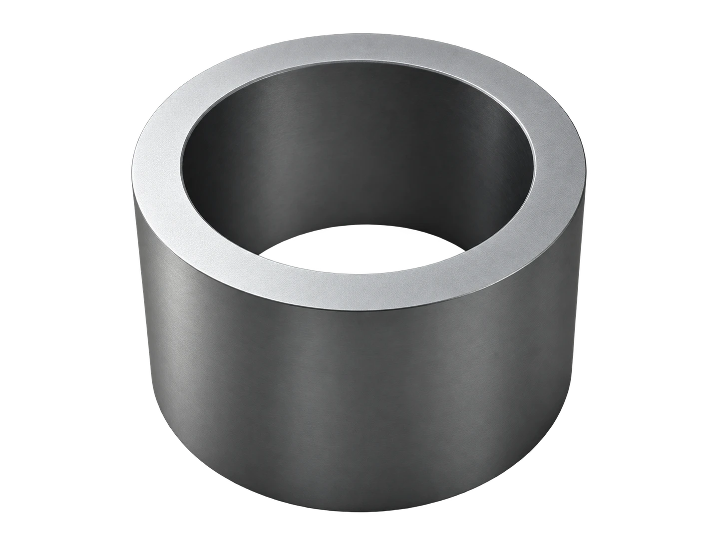
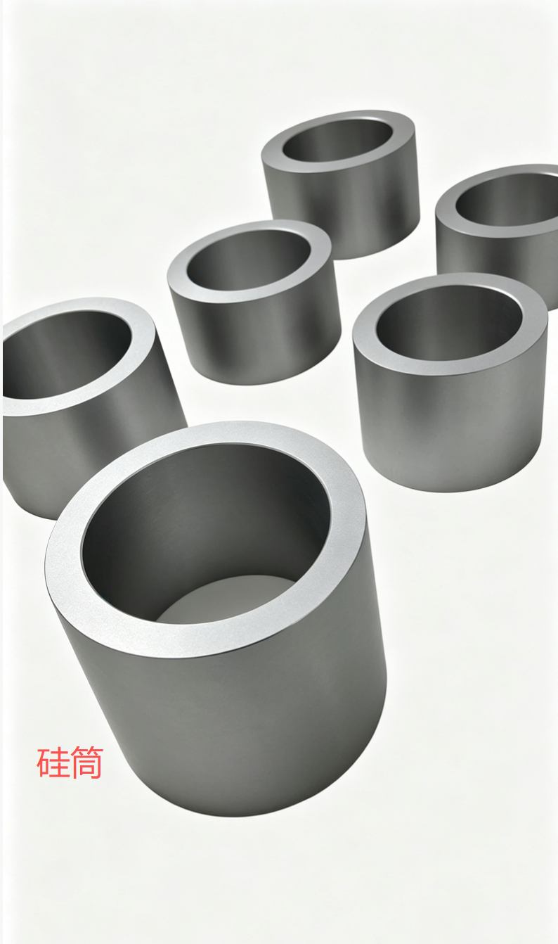
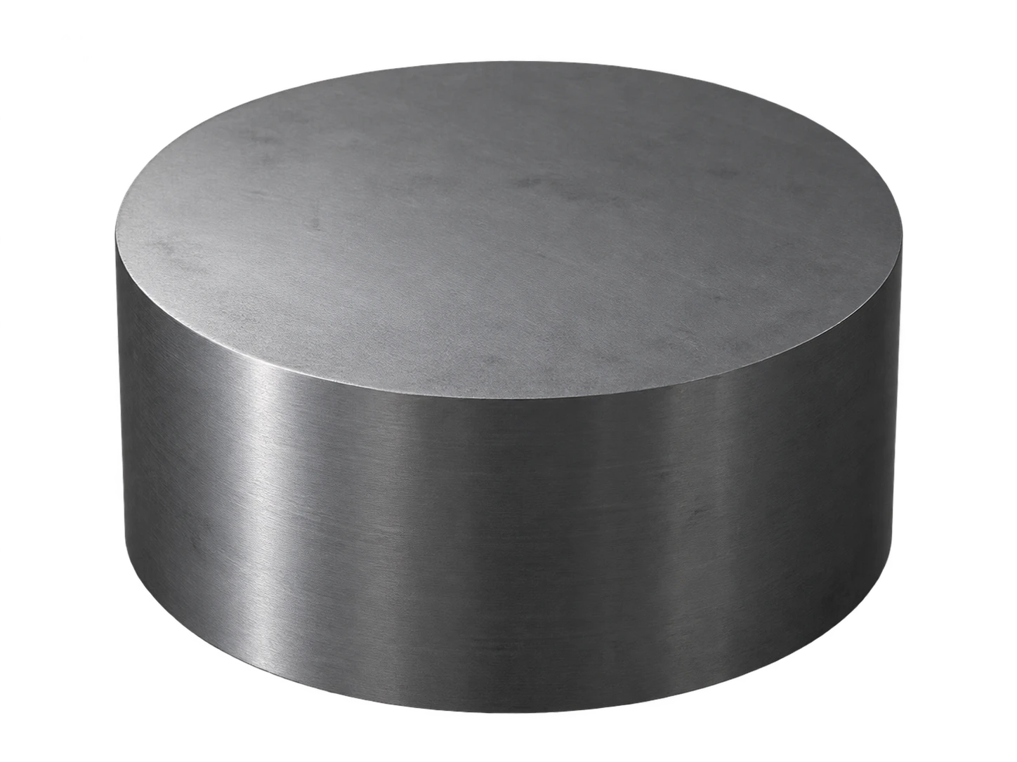
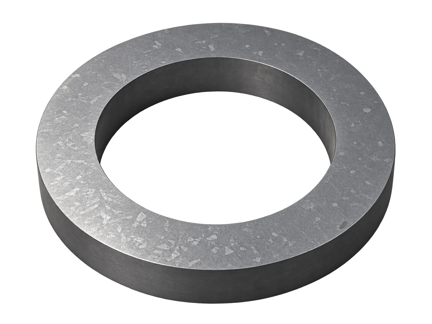
Cored and formed cylindrical material provides blanks for silicon ring components used in etching.
Conductivity type, resistivity, dimensions and surface condition can be confirmed for the specific application.
Product Photographs
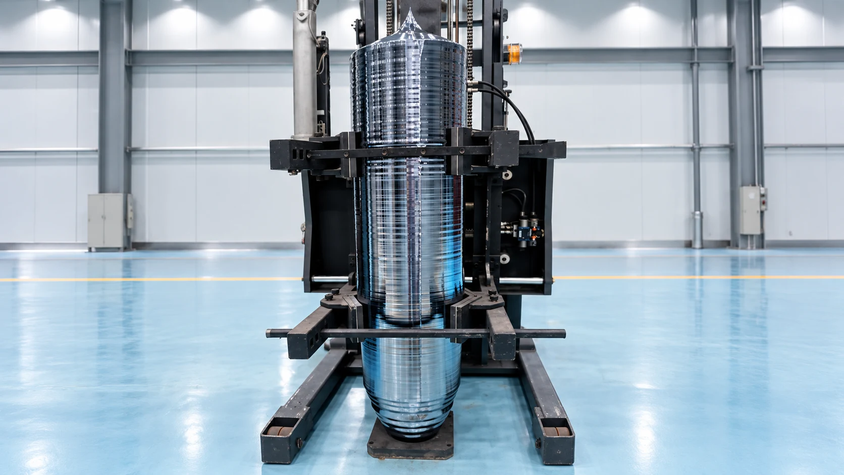
Actual product photographs. Delivered dimensions and surface condition are subject to drawings and the technical agreement.
Material specifications for silicon etch components
Monocrystalline Silicon Ingots
Monocrystalline Silicon Cylinders
Monocrystalline Silicon Rings
Material type
Monocrystalline silicon
Monocrystalline silicon
Monocrystalline silicon
Principal sizes
450–600 mm (specific sizes subject to technical agreement)
450–600 mm (specific sizes subject to technical agreement)
450–600 mm (specific sizes subject to technical agreement)
Purity
>8N
>8N
>8N
Conductivity type
P-type (boron) / N-type (phosphorus)
P-type (boron) / N-type (phosphorus)
P-type (boron) / N-type (phosphorus)
Resistivity
<0.02、1–4、60–90 Ω·cm
<0.02、1–4、60–90 Ω·cm
<0.02、1–4、60–90 Ω·cm
Dimensional tolerance
Within ±0.05 mm
Within ±0.05 mm
Within ±0.05 mm
Flatness
≤15 μm; high grade ≤8 μm
≤15 μm; high grade ≤8 μm
≤15 μm; high grade ≤8 μm
Surface roughness
Standard Ra≤0.4 μm; polished Ra≤0.1 μm
Standard Ra≤0.4 μm; polished Ra≤0.1 μm
Standard Ra≤0.4 μm; polished Ra≤0.1 μm
Product specifications, inspection methods and delivery condition are governed by mutually approved technical agreements and drawings.
Large-Diameter Crystal Growth
Our focus is large-diameter products, an integrated technical process and continued process development. Alongside stable production of 450 mm diameter products, we are developing and evaluating processes for 600 mm and larger products.
Material Forms & Machining
From monocrystalline silicon crystals to solid, cylindrical and ring blanks, machining routes and material requirements follow component drawings.
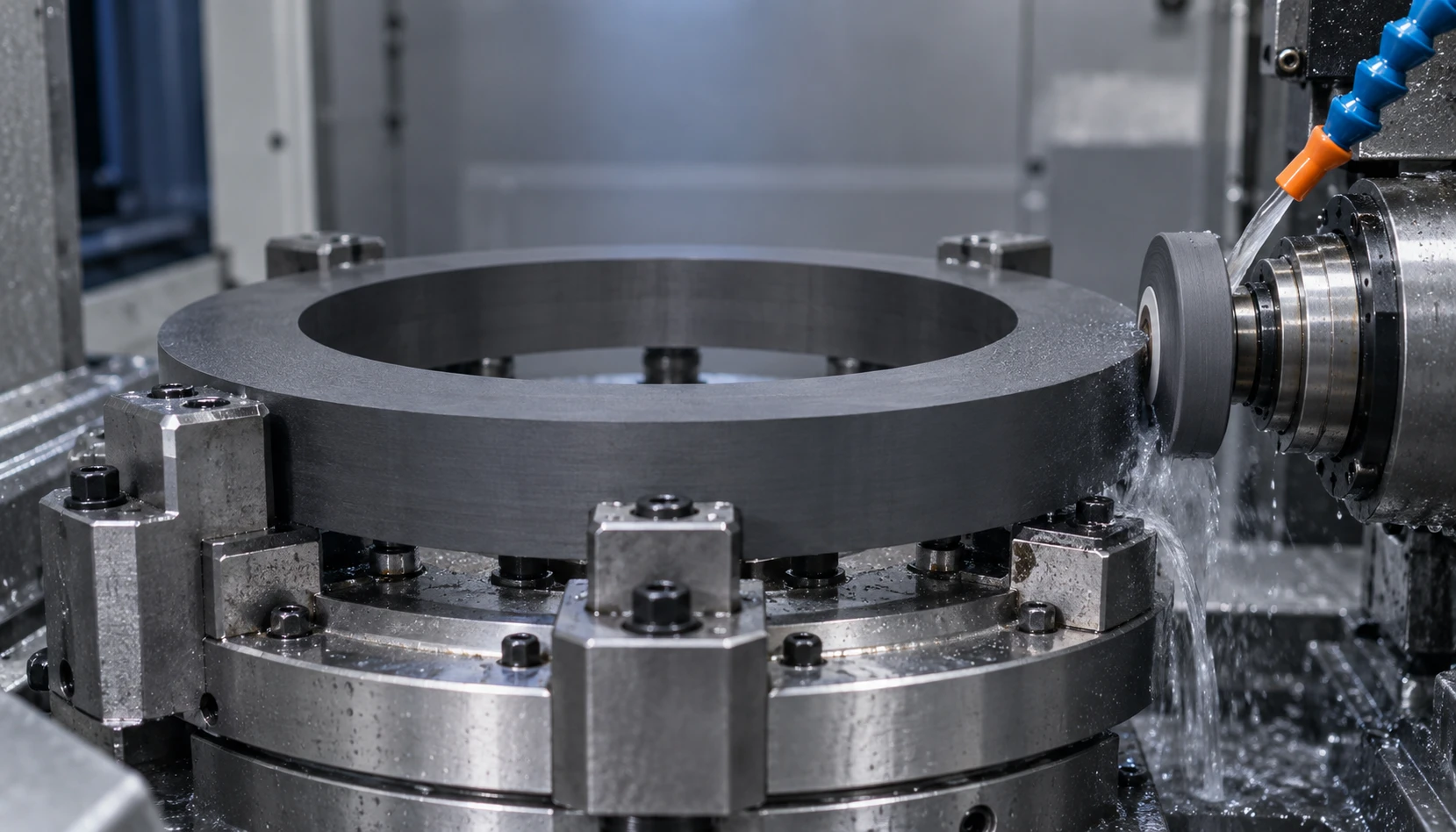
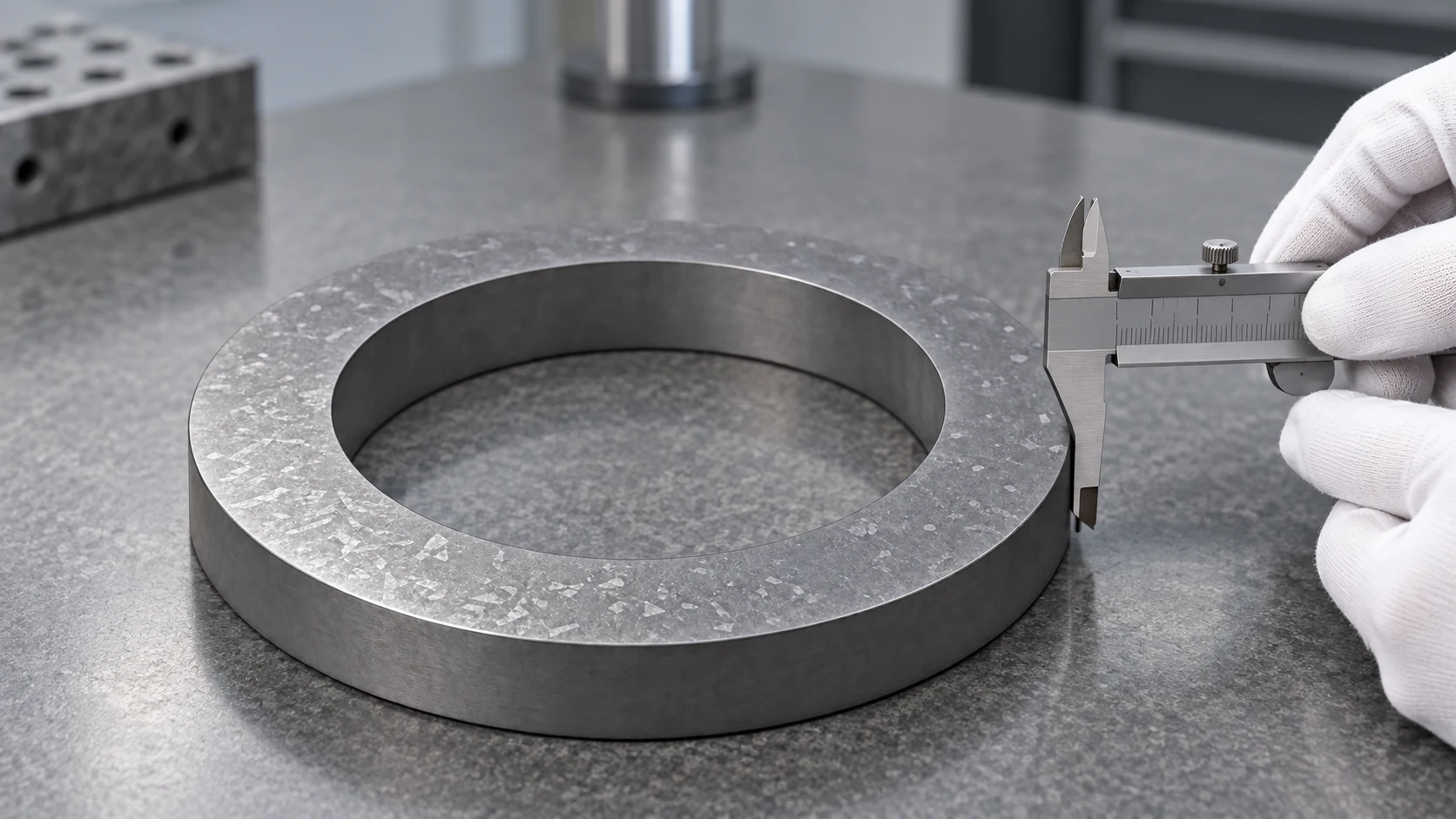
Confirm outer and inner diameters, thickness and critical geometric tolerances against etch-component drawings. Grind and precision-machine the selected material form, then inspect according to the technical agreement.
Precision machining
Dimensional inspection
Downloads
Silicon Materials for Semiconductor Etching — Product Guide
We connect large-diameter crystal growth with downstream machining. Material properties, critical dimensions, surface condition and inspection documents are confirmed against project drawings and technical agreements.