ABOUT US
Company Overview
Silicon materials for semiconductor etching: research and manufacturing
Established in September 2023 in Daxing, Beijing, Jonkin Silicon supplies large-diameter monocrystalline silicon, machining and custom development services to silicon etch-component and related equipment manufacturers.
OUR BUSINESS
Core Business
Material Supply
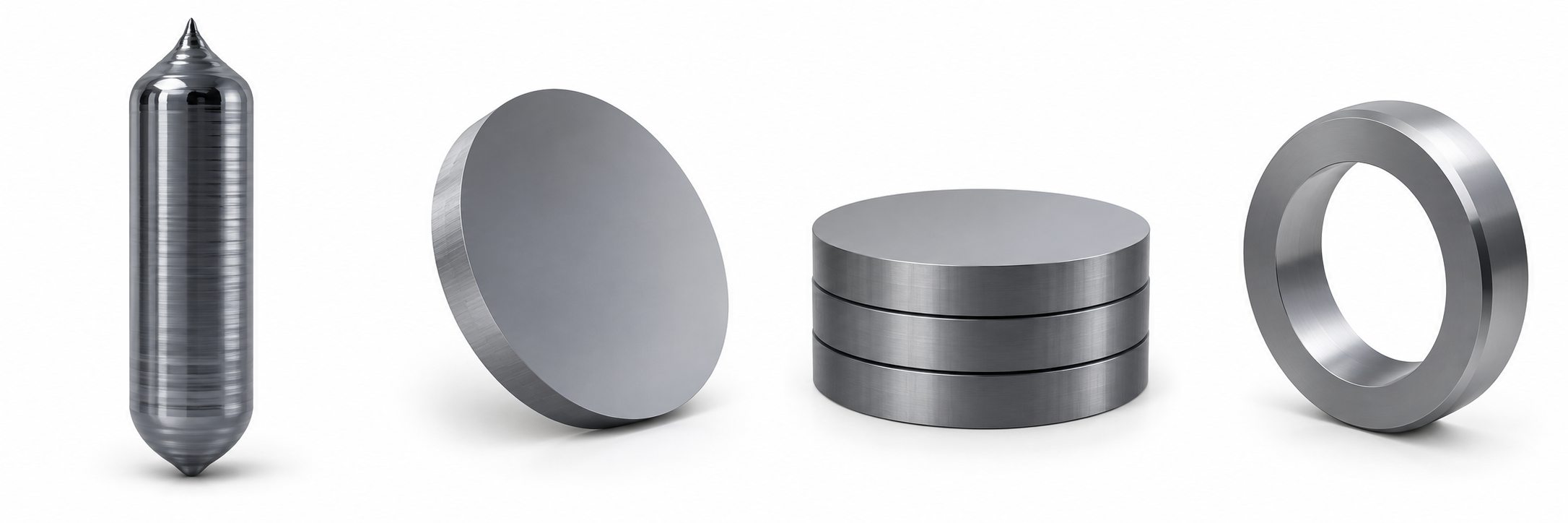
Silicon ingots, cylinders and rings
Large-diameter monocrystalline silicon, with material properties and delivery forms defined for component applications.
Manufacturing
Machining routes and delivery condition defined by drawings
Cutting, grinding and precision machining to target dimensions and surface requirements.
Custom Development
Collaborative development for equipment and component needs
Material applications and machining processes developed from material requirements and technical drawings.
TECHNOLOGY
Technical Capabilities
From Crystal Growth to Precision Machining
Our technical process connects crystal growth and machining, aligning development and manufacturing with component dimensions, surface condition and material properties.
CZ Crystal Growth
Cutting
Grinding
Precision Machining
450 mm
Stable Production
Stable production of 450 mm diameter products has been achieved, supplying customers with large-diameter material.
600 mm and Above
Development Direction
Continued material development and process evaluation for larger-diameter requirements.
OUR TEAM
Team & Experience
The project founder has over 20 years of industrial manufacturing experience and more than six years in senior management at a listed company, with experience in production, supply and sales management for semiconductor wafer preparation, crystal growth and equipment machining.
Our technical team has industry experience across crystal growth, cutting, grinding and precision machining, using close collaboration to connect material development with engineering and manufacturing.
MILESTONES
Milestones
2023.09
Company Established
Jonkin Silicon was formally established.
2025.02
Crystal-Growth Milestone
A 440 mm diameter monocrystalline silicon rod was successfully grown using the CZ method.
2025.08
Recharging Process Milestone
Crystal-growth recharging trials succeeded.
2026.02
Hot-Zone Trials
36-inch hot-zone trials were completed, advancing process validation for large-diameter products.
2026.04
Large-Diameter Development
Development of 600 mm diameter products began.
OUR PLAN
Development Plans
Planned Targets
Focused on silicon etch-component and related equipment manufacturers, the company plans an initial three production lines with a target annual output of 35 tonnes of monocrystalline silicon, allowing room for expansion with customer demand.
These are planned targets, not claims of existing production lines or actual annual output.

PARTNERSHIP
Partnership & Vision
Advancing Domestic Semiconductor Materials with Industry Partners
Guided by technology and market needs, we aim to be a reliable supplier of silicon materials for semiconductor etching. We welcome collaboration in material supply, manufacturing and custom technology development.